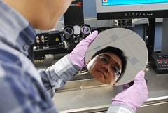
Researchers at IBM Corporation’s Thomas Watson research lab in New York developed a method for assembling high densities of carbon nanotubes on a wafer surface, a key advance in fabricating semiconductors. The IBM team led by Hongsik Park (picured right) published its findings yesterday online in the journal Nature Nanotechnology; paid subscription required.
Carbon nanotubes — tiny nanoscale cylinders of single carbon atomic sheets, where 1 nanometer equals billionth of a meter — have the potential to replace silicon as the basic material of semiconductors, because of their superior atomic shape and ability to transfer data. Up to now, however, researchers have been able to place at one time a few hundred carbon nanotube devices, not nearly enough for commercial applications.
Among the challenges faced by the IBM team is that carbon nanotubes are not naturally in a pure state, but instead start out as a mix of metallic and semiconducting materials. For a semiconductor device to operate properly, only the semiconducting material is useful, which requires removing the metallic content to prevent errors in the circuits. Also, to make large scale integration possible — an essential requirement for semiconductor fabrication — the alignment and location of carbon nanotube devices on a substrate must be carefully controlled.
The IBM researchers devised a process that adapted a form of ion-exchange chemistry to remove dissolved ions from a solution through electrostatic attachment. In this case, the team used a surfactant that acts like soap to suspend materials in fluid, to deliver the carbon nanotubes to a wafer substrate made of chemically-modified hafnium oxide and silicon oxide. The researchers immersed the substrate in the carbon nanotube solution and found the nanotubes to bind chemically with the hafnium oxide regions of the surface while the rest of it remains clean.
The researchers report that this process allows for precise and controlled placement of aligned carbon nanotubes on a substrate at a high density, of some one billion nanotubes per square centimeter. In their experiment, the team was able to place carbon nanotube transistors in a conventional semiconductor fabrication line, with more than ten thousand transistors placed and tested on a single chip.
“Carbon nanotubes, borne out of chemistry, have largely been laboratory curiosities as far as microelectronic applications are concerned,” says Supratik Guha who directs IBM’s research in physical sciences. “We are attempting the first steps towards a technology by fabricating carbon nanotube transistors within a conventional wafer fabrication infrastructure.”
Read more:
- Rice, NIST to Partner on Nanoscale Carbon Materials Research
- Carbon Nanotubes Found Toxic to Aquatic Animals
- Nanotubes Boost Biosensors for Faster Medical Diagnostics
- Solid-State Supercapacitor Created with Carbon Nanotubes
* * *
