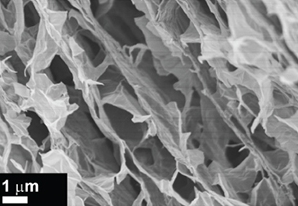
17 October 2014. Materials scientists at Kyoto University in Japan developed a new process that simplifies the building of three-dimension structures with graphene, a light, strong, conductive material with many industrial and commercial applications. Franklin Kim and Jianli Zou from Kyoto’s Institute for Integrated Cell-Material Sciences published their findings yesterday in the journal Nature Communications (paid subscription required).
Graphene is a material closely related to graphite like that used in pencils, but consists of only a single layer of carbon atoms arrayed in a hexagonal mesh pattern. The material is very light, strong, chemically stable, and can conduct both heat and electricity, with applications in fields such as electronics, energy, and health care.
The thin, single-atomic structure that makes graphene a desirable material also makes it difficult to piece together into 3-D structures needed for practical use, which hampers the advance of graphene into commercial applications. Stacking graphene layers, for example, causes the nanoscale sheets to lose their unique individual properties. Current methods for addressing this problem, say the authors, are costly and time consuming.
Kim and Zou sought a simple and scalable method for assembling graphene sheets that can be adapted to commercial and industrial enterprises. The researchers applied a chemical process known as interfacial complexation, where layers of negatively-charged graphene oxide sheets are interspersed with a positively-charged polymer. The polymer in this case is polyethylenimine, a compound used in detergents, adhesives, inks, dyes, and cosmetics, as well as a number of industrial processes.
Putting the opposite-charged layers of graphene oxide and polyethylenimine into contact forms a stable composite layer. “Interestingly, the polymer could continuously diffuse through the interface, and induce additional reactions” says Zou in a university statement, “which allowed the graphene-based composite to develop into thick multi-layered structures.”
The multi-layered structures, say the authors are robust and can be designed with various porosity, from ultra-light to extremely dense, by adjusting the input properties and conditions. The process can be scaled easily for producing large-area films with patterns, or into free-standing shapes for energy generation or storage, such as in batteries or supercapacitors.
Kim adds that the process can be applied to more than just graphene, noting “we strongly believe that the new technique will be able to serve as a general method for the assembly of a much wider range of nanomaterials.”
Read more:
- Graphene Sensor Designed for Wearable Disease Detection
- Epoxy/Carbon Ink 3-D Printed into Lightweight Cell Material
- Industrial Scale Graphene Production Process Devised
- Pressure-Cooked Nanoparticles Improve Lithium-Ion Batteries
- Consortium Funds Bio-Semiconductor Component Research
* * *
