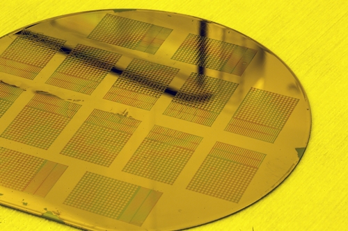
29 October 2015. Engineers at University of California in San Diego developed a process that simplifies production of flexible electronic sensors worn on the skin for medical diagnostics. The team from the lab of bioengineering professor Todd Coleman published its findings in a recent issue of the journal Sensors.
The UC-San Diego team was seeking ways to reduce the time, complexity, and cost of producing thin, flexible sensors worn on the skin that can monitor vital signs and other indicators of disease. With large-scale growth expected in wearable devices and Internet-of-Things applications, the market for these flexible systems seems immense. Prototype skin-patch sensors produced in the lab show these devices are technically feasible, but they are so far produced individually or in small numbers.
The current process for making these sensors, note the authors, requires 10 separate steps, using a clean room with equipment similar for producing semiconductors. Just removing finished sensors from a silicon wafer, for example, could take up to 20 minutes. In addition, the finished product was often too fragile and tore too easily for practical use.
Coleman’s lab already has experience working with medical professionals, and sought the advice of nurses, the people most likely to use these stick-on sensors in the clinic. The researchers found nurses preferred a product they could peel off from a substrate, like a band-aid, and apply directly to a patient. Their inquiries also revealed any system for dispensing the sensors needed to use materials that the Food and Drug Administration already approved.
Graduate student Dae Kang developed the process described in the journal paper. That process fabricates the gold and chromium sensor circuits on a layer of flexible organic polymer known as polydimethylsiloxane, also known as PDMS or silicone, a material used today in breast implants. The photo-sensitive silicone layer is 20 to 50 micrometers thick, where 1 micrometer equals 1 millionth of a meter.
With the requirement for a peel-off dispenser, the team had to make the silicone layer sticky enough to hold the circuits in place, yet still be easily removed. The researchers found they could print the circuits directly on the silicone layer, stiffening the surface somewhat to allow printing the circuits, and apply a flexible transparent adhesive film on top. The circuits could then be removed from the silicone layer with the adhesive film.
The researchers tested the process using simple, readily-available adhesive films including, for example, an ordinary lint roller. Tests of the sensors themselves show they work equally as well as skin-patch sensors produced using current methods, connecting to an electroencephalogram or EEG measuring brain activity with a sensor applied to the forehead, and electrical activity in the heart with an electrocardiogram or EKG.
Kang’s process succeeded in simplifying production of these skin-patch electronics from 10 steps to 6, with only 3 of the steps requiring a clean room, and cutting end-to-end production time in half. The time needed to remove sensors from the wafers was reduced from as much as 20 minutes to about 35 seconds. As important, the process of directly fabricating the circuits on the silicone substrate makes it feasible to use roll-to-roll industrial printing methods, which would mean much lower costs when produced on a commercial scale.
Students in Coleman’s lab demonstrate the process in the following video.
Read more:
- Heart-Powered Leadless Pacemaker in Development
- Spin-Off to Provide Lower-Cost Molecular Imaging Technology
- Chip Device in Development to Simulate Human Gut
- Nanotech Cancer Center Gains $10.1M Funding
- Manufacturing Process Devised for Skin-Patch Electronics
* * *
